What's New?
Latest updates March, 2019. The main links at the top of the page describe different sections of the site. Check this area for changes.
Useful links
The links below should make it easy to find software and stuff related to most of the projects on this site.
Circuits and Printed Circuit Boards
Circuits, silkscreens and enclosures, Oh my!
What's the process for making really nice looking PCB's and enclosures?
Your process depends on your intentions for the circuit.
One board, never to be made again. If you are making a one off board with few traces and large pads, then you could always use the old-fashioned sharpie method. With this method, you simply draw the entire circuit on the copper side of the board by hand, and then etch your board. Nice looking? not so much, but it'll probably work if you drew solid lines.
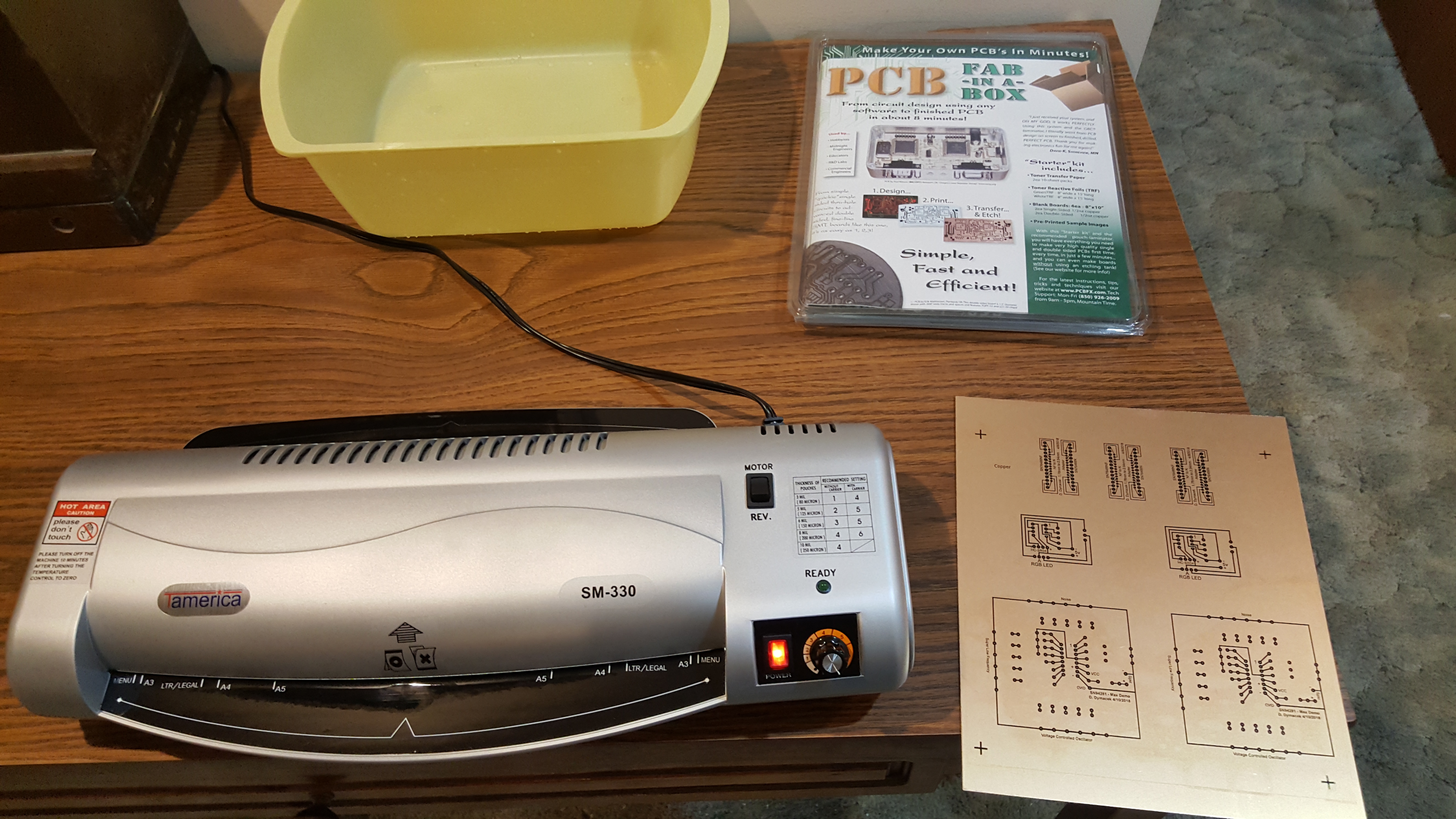
Another method for making one off boards is a kit like "PCB Fab-in-a-box". This method uses special transfer paper (with black and white TONER-TYPE printers or copiers only), and will produce some great results. The toner type printer or copier is a must to use this kit, and the transfers won't work with any other type of printer.. not wax, not inkjet. HP is highly recommended due to the toner composition. An iron can be used for the transfer to your copper layer, but the manufacturer recommends a laminator, which I have. I also use the laminator for the enclosure panels. It might seem like I'm advertising for them, but I'm not. This is just the easiest way that I've found to make your own circuit boards at home.
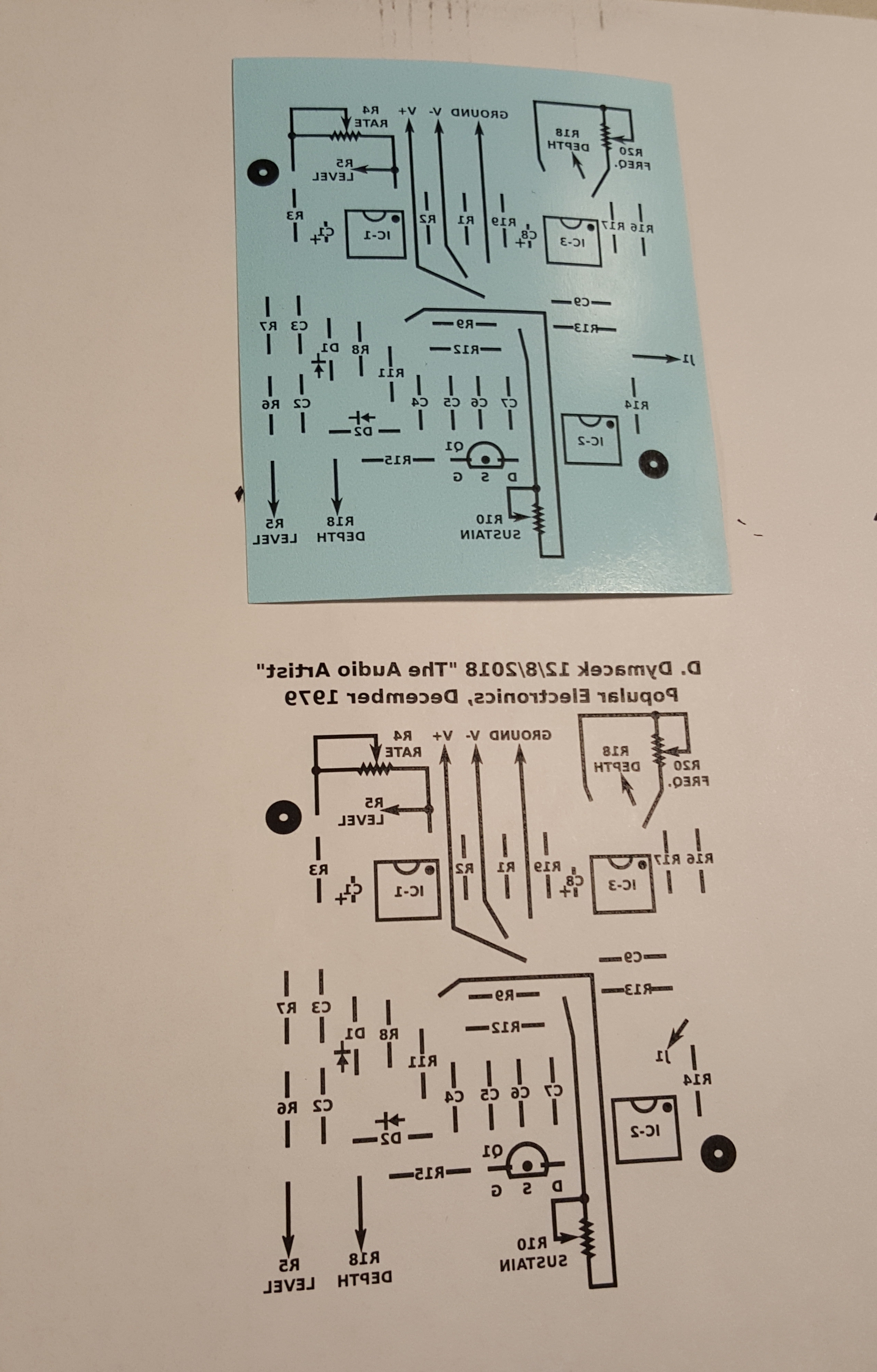
If you are making a single sided board with no silkscreen, this is a pretty easy process with transfers. Use your favorite vector graphics software (like Inkscape) to draw the circuit looking from the component side. Make sure to reverse any text you want on the copper side, and then print on the transfer paper, fuse the transfer to the copper and etch.
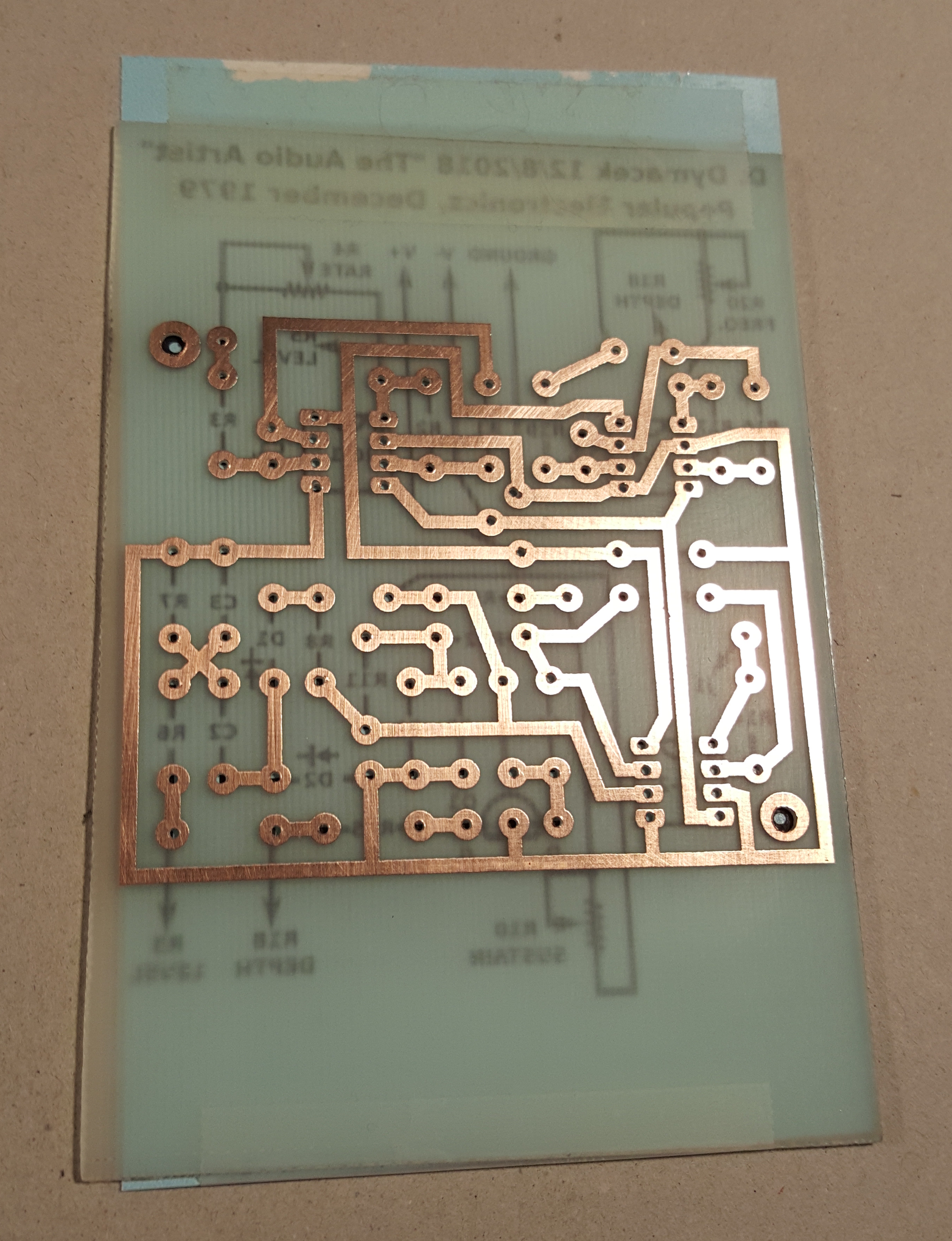
The reason that the circuit traces are from the component side and the text is reversed is because the transfer process reverses the image. Once printed, if you hold the print to a light and LOOK THROUGH the paper, you will be looking at the copper side of the board, and able to read all of the text. Looking at the printed side of the paper is basically like looking at the component side of the board. What you see is on the other side of the board, on the copper. It's a little confusing at first, but when you try it it becomes more clear. Adding a silkscreen layer is another level of confusion, but its easy once you know how.
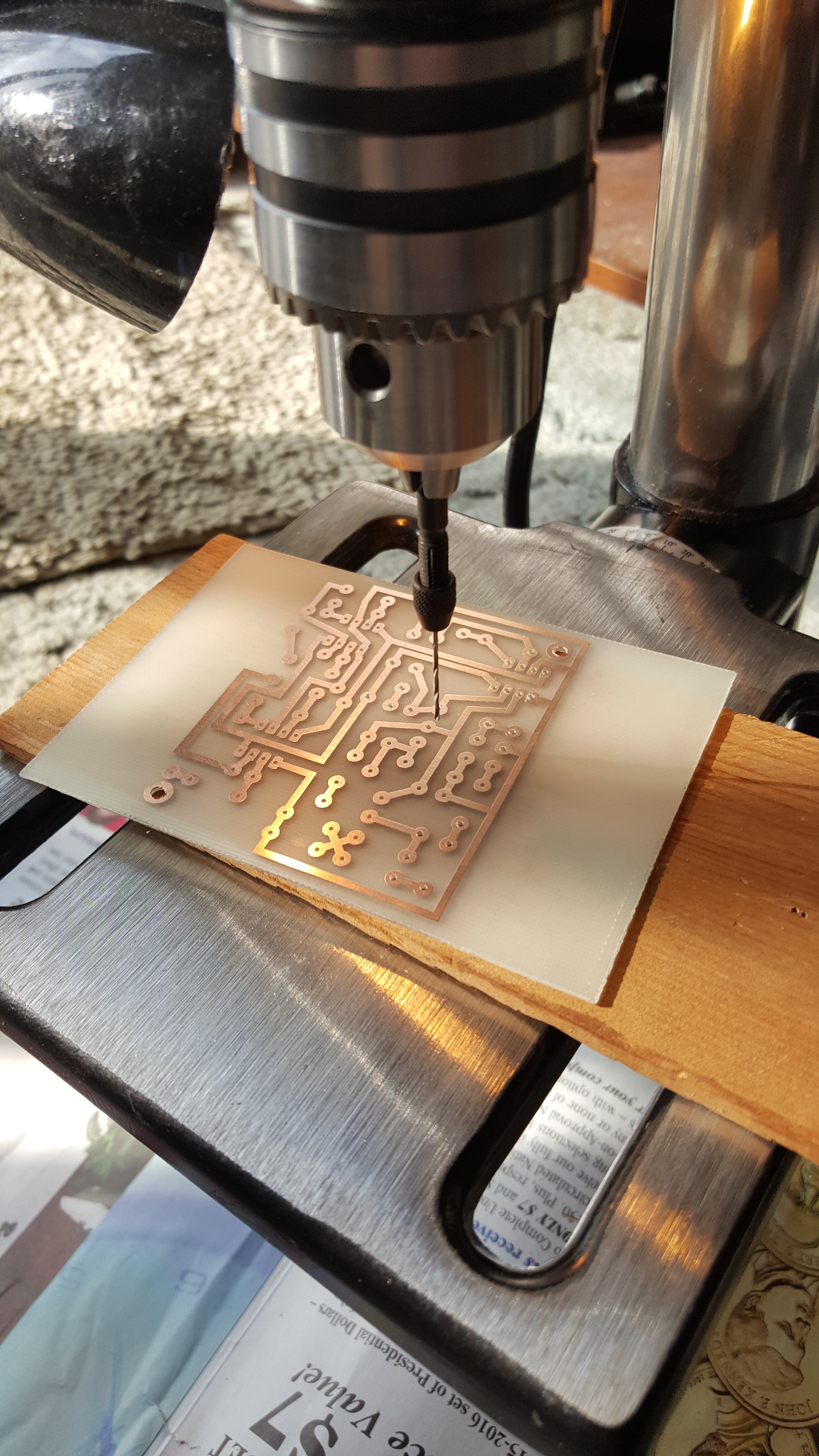
And then you'll have to drill all of the holes.. On more dense boards, this takes patience and practice.
You can also send your schematics to a third party and they'll make your boards for you. This is the most expensive option for a single board, but still less expensive than a transfer kit if this is the last board you'll make (actually, you could get about 4 professionally made PCB designs for less than the kit, laminator and printer). Many of these companies require you to create your schematics or drawings using specialized or proprietary software, so you'll need to learn that too. Very few PCB companies let you use vector graphics software you are familiar with (like CorelDraw, Adobe Illustrator or Inkscape), and some of these proprietary programs are not trivial to learn.
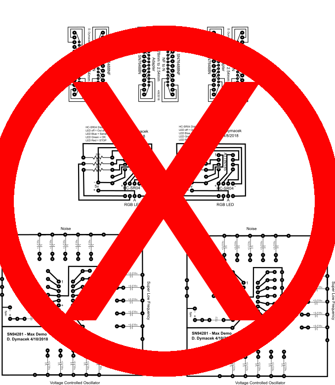
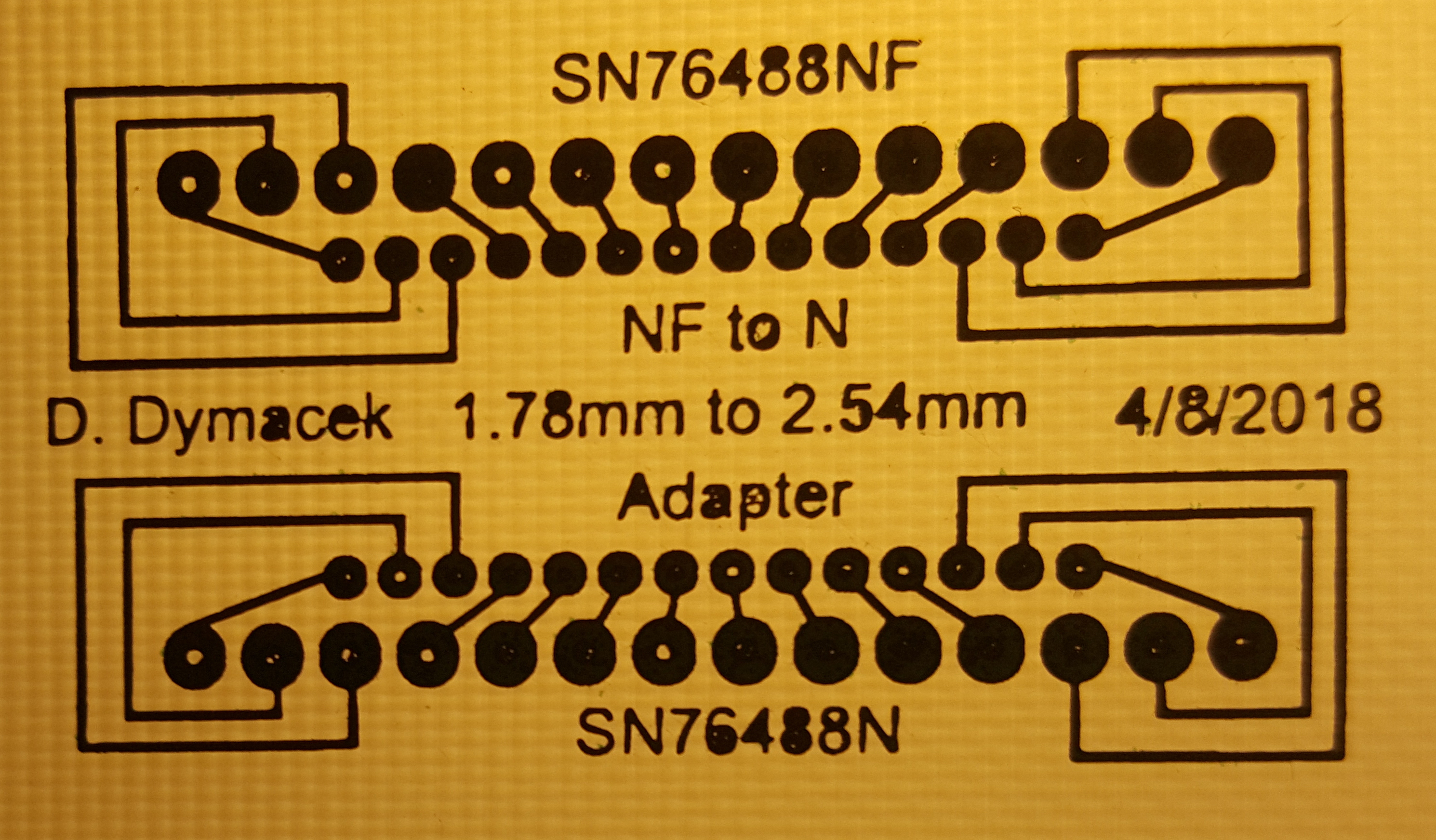
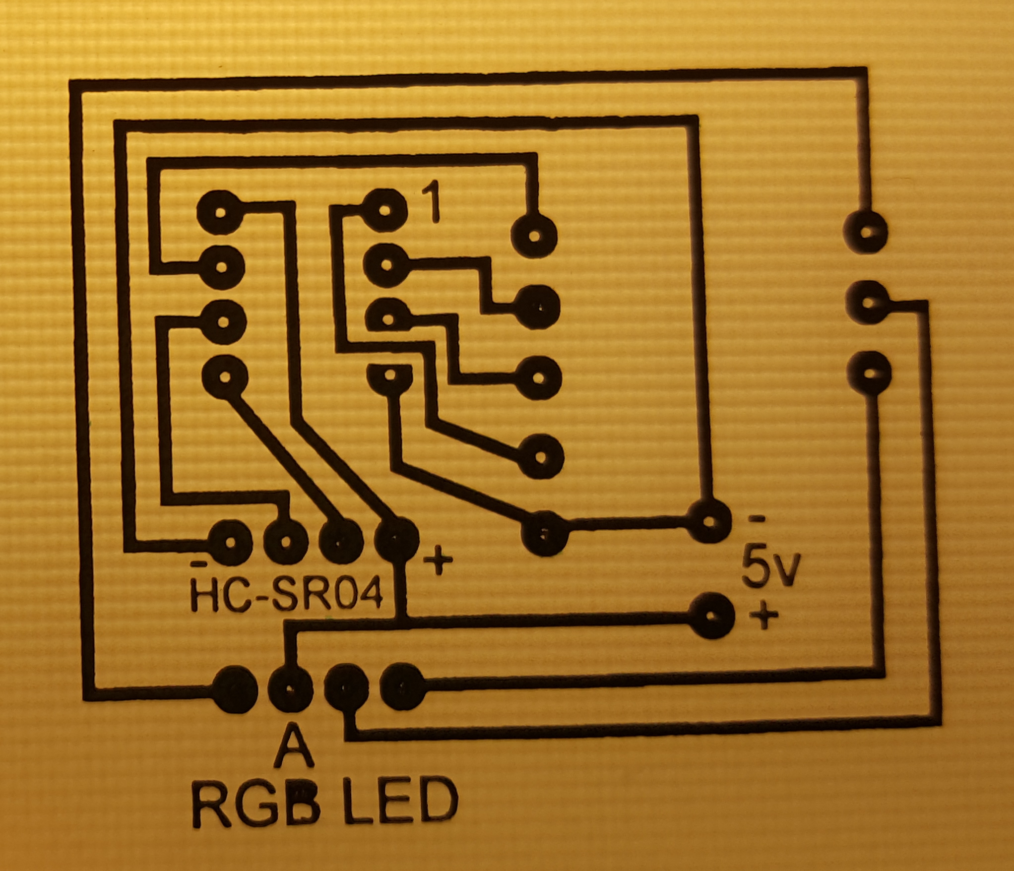
The image at the top-left of this page is NOT printer ready. It's actually the copper side and silkscreen as viewed from above, as if the board were clear. I made a few of my own PCBs in the distant past (30+ years ago), but this was my first attempt using PCB-Fab-In-A-Box, and wow I learned a lot making these boards. One thing was that I should have made multiple sets rather than one large board. SVG images of the three different circuits split into sepatate files are below.
Printing your own PCB's

Print your own PCB's! It's fun.
Well, fun might be the wrong word. It's actually a pretty challenging thing to do the first time, but the process gets easier once you understand what needs to be reversed on which layers of your drawing.
Isn't there some really easy way to make my own boards? Well, no. Not really easy. If you can learn new software quickly, then the first time will be the most difficult, and it will get easier from there.
Once upon a time, there were rub off transfers in the shapes of IC chip pads, wire traces, and other components, and you would carefully position them on your copper board and use a pencil to rub the transfer onto the copper. This was not a difficult process, but it was really time consuming, and fingerprints didn't help. I've also used the sharpie method for really simple boards, but it's been a while.

I am currently using the "PCB Fab-in-a-Box" method mentioned above, and it works spectacularly for my projects. The most difficult part of this process (to me, so far) was understanding what needed to be reversed on the page. In the end, it comes down to this.. Draw the copper layer as if looking at the component side, and draw the component side normally, and then reverse it. Again, it gets easier once you do it. Looking through the printed pages imagining a board in the middle helps. Once you've got your image done, you can make a bunch of the same boards easily.
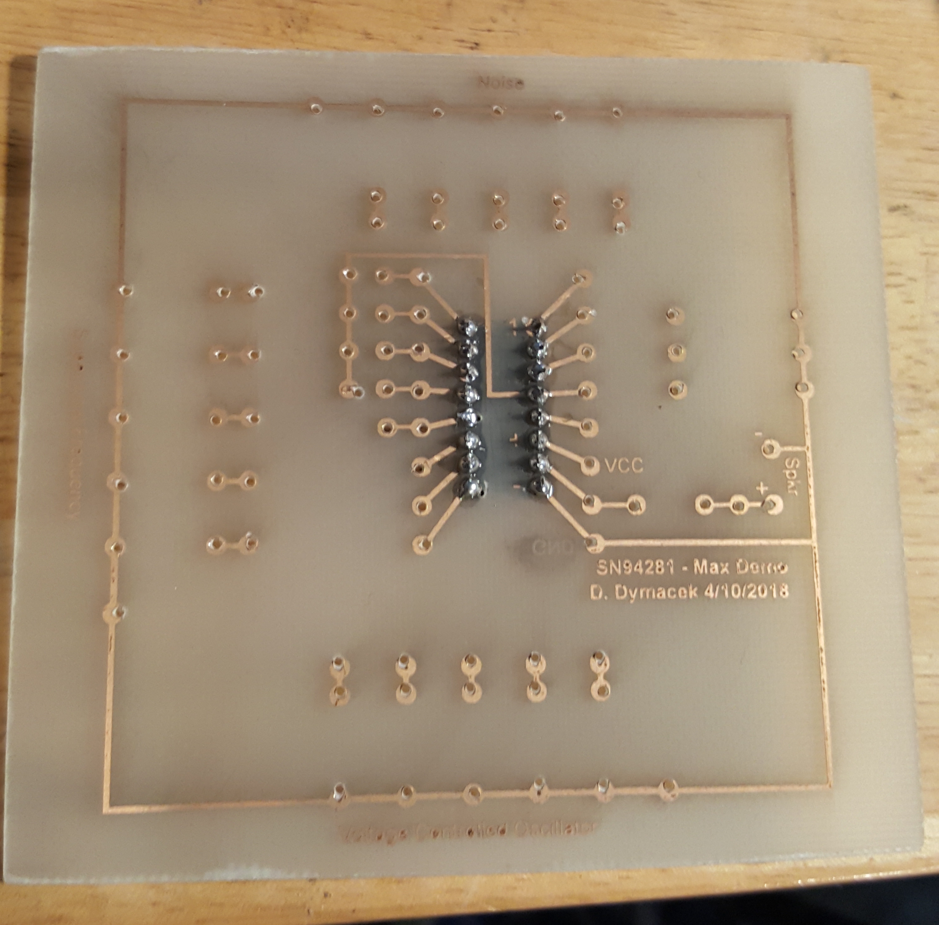
Eventually I realized that I didn't even need to do both layers at the same time, and that registering both layers (getting them to line up accurately with each other without being able to see through the board) would require drilling a few holes through the copper layer after it was finished anyway.
This isn't even what the pcb-fab people recommend unless you're making a double sided board, which I'm not. The recommended method is to etch the copper side, drill your holes, and THEN add the silkscreen layer. Since the boards are mostly translucent, you can see through them, and lining up everything works much better this way.
The image at the upper left of the page (with the x through it) was what I originally used, but it was separated into separate files to make it easier to download and use. The original run made 7 total boards in 3 different designs. I made a few extra boards in case I needed them later, AND because it's easy to make additional boards once they're drawn. These boards have all been built and work as expected. There is at least one mistake on there, and it's a bit of reversed text that shouldn't be. I'm better at it now. :-)
Lessons learned from my first attempt with PCB Fab-in-a-box.

I wasted lots of space on my transfer paper, TRF foils, and copper board. I have no idea why I thought printing all of the circuits on a larger board would be the way to go, but as it turns out, smaller is better. The transfer paper is 8.5x11, so I think that fooled me into believing I needed to use that size.
The best process I've found is to print your image on regular paper, cut your transfer paper slightly larger than the image on the page, tape your tansfer paper over your printed image, and print again. Make sure you leave enough space around the edges of the transfer paper for your tape.
You'll need to cut and drill your boards too. I thought that I could use my router table with a thin bit, but the table wasn't really made for small pieces, and I ended up using a razor knife and straight edge to score and snap the boards apart. This leaves a pretty rough edge, and you'll also need to clean that up.
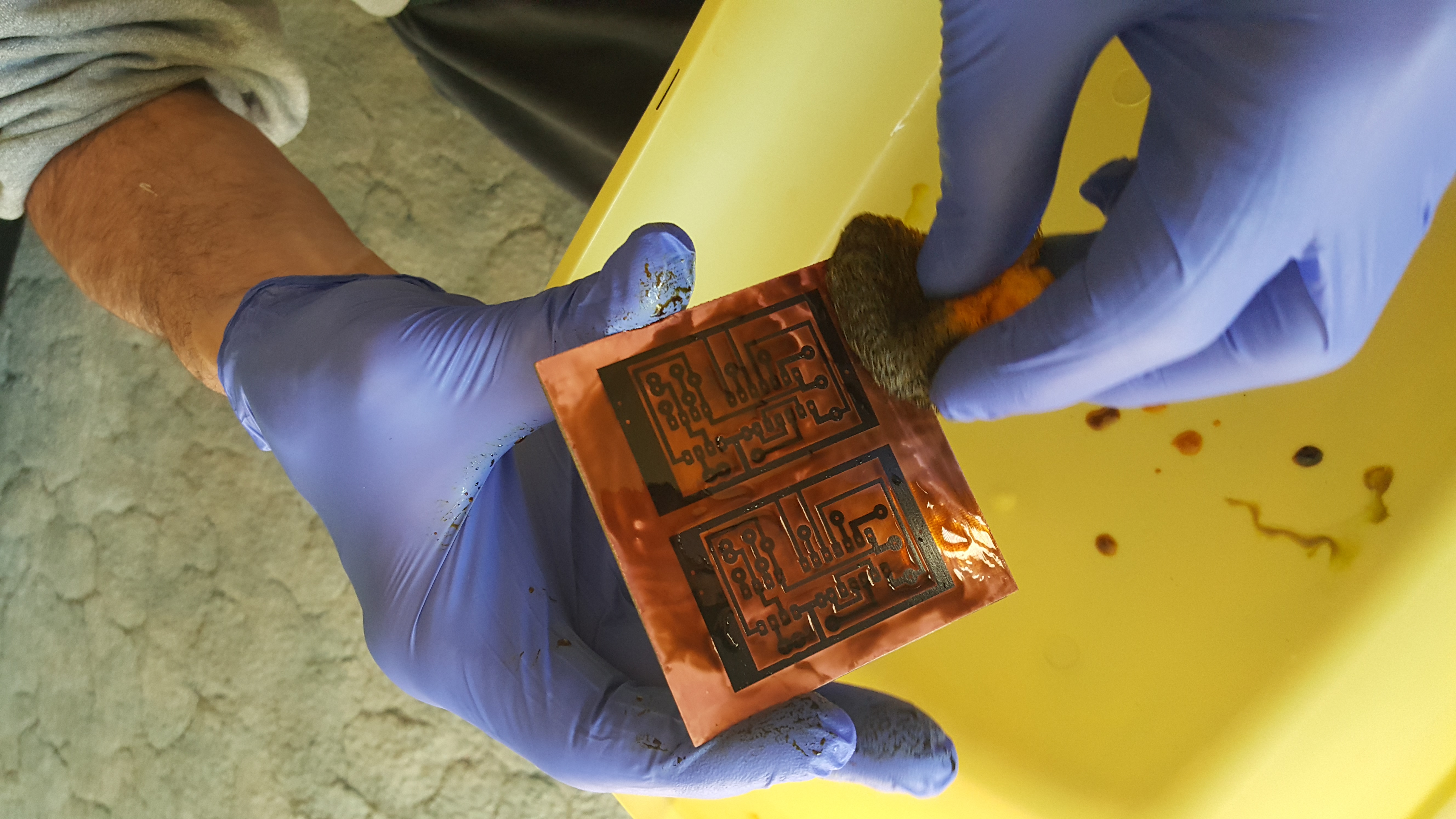
You can etch your boards with a sponge or cotton ball! One of the tips from the PCB Fab site is using a sponge (wearing gloves of course) to etch the circuit board using a minimum quantity of etchant (in my case ferric chloride). Basically, you just liberally wet the sponge with etchant and wipe the copper off the board. It only takes a minute or so, and I was surprised how well it worked. I had already poured about 3/4 of a cup of solution into my etch tank before I remembered to try this, but that's all the solution I used. Now I've got it down to a few teaspoons of etchant per batch, and I just roll the cotton ball up in my rubber gloves and throw it away.
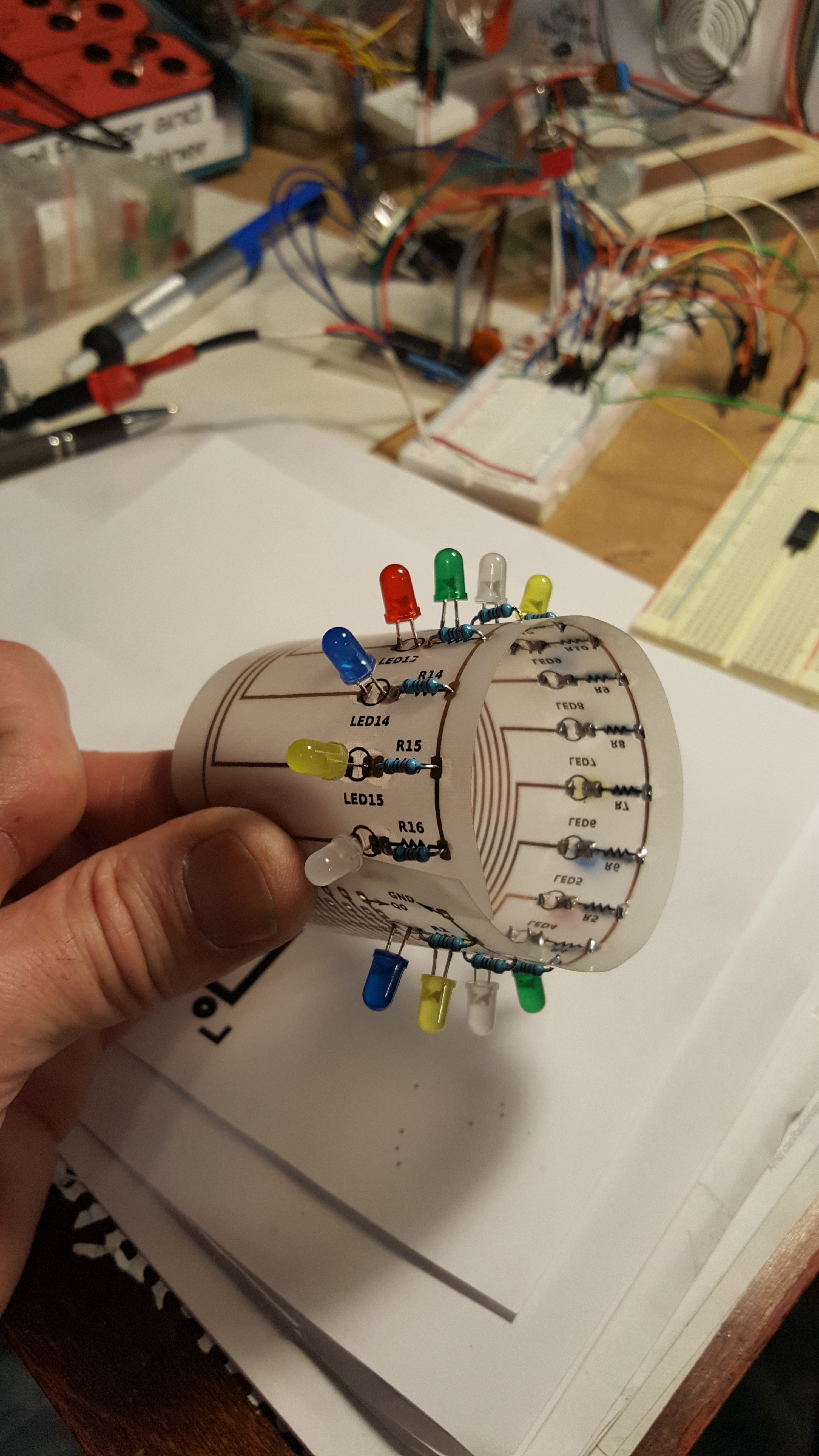
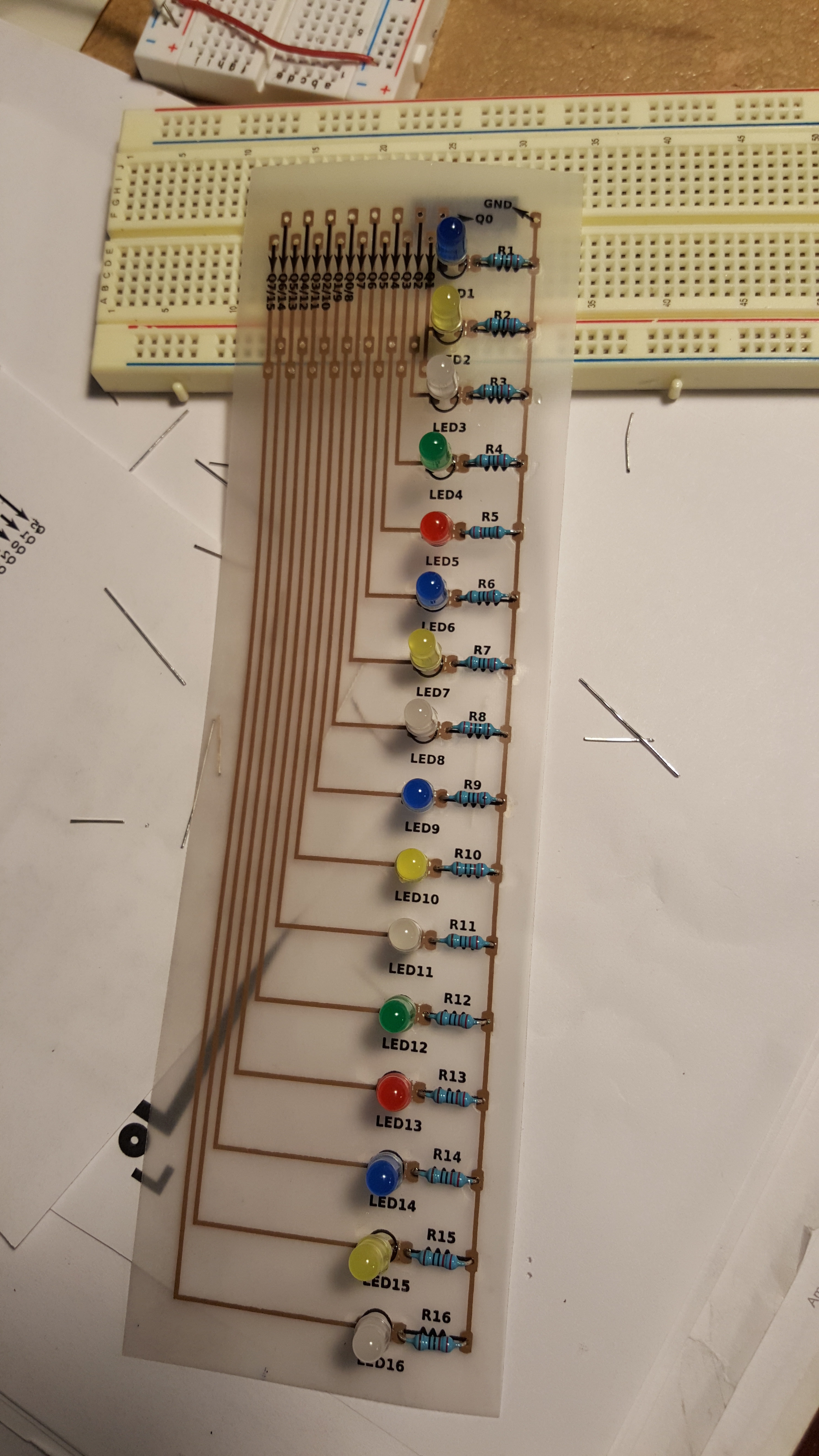
In the end, I was pretty happy with my first try using this "technology". The copper side came out perfect (with the exception of a little acetone smear), and the silk layer was pretty close. I lost a few letters because either I had finger oils on the board before transfer, or didn't run it through the laminator enough.
At this point I can complete a small board in a few hours, from a schematic to PCB and silkscreen design to etching and drilling. Practice really does help, and this kit makes it simple to make lots of boards!
I've even made my first flexable PCB, and it was easier than I thought it would be. I really didn't make the best application of the flexable circuit, but I hadn't made one before, and was really just curious what to expect. I can see using these for custom connectors between boards, but to do that, you'd need specialized parts. I could easily imagine making electronic oragami with the flexable board.
A nice PCB deserves a nice enclosure
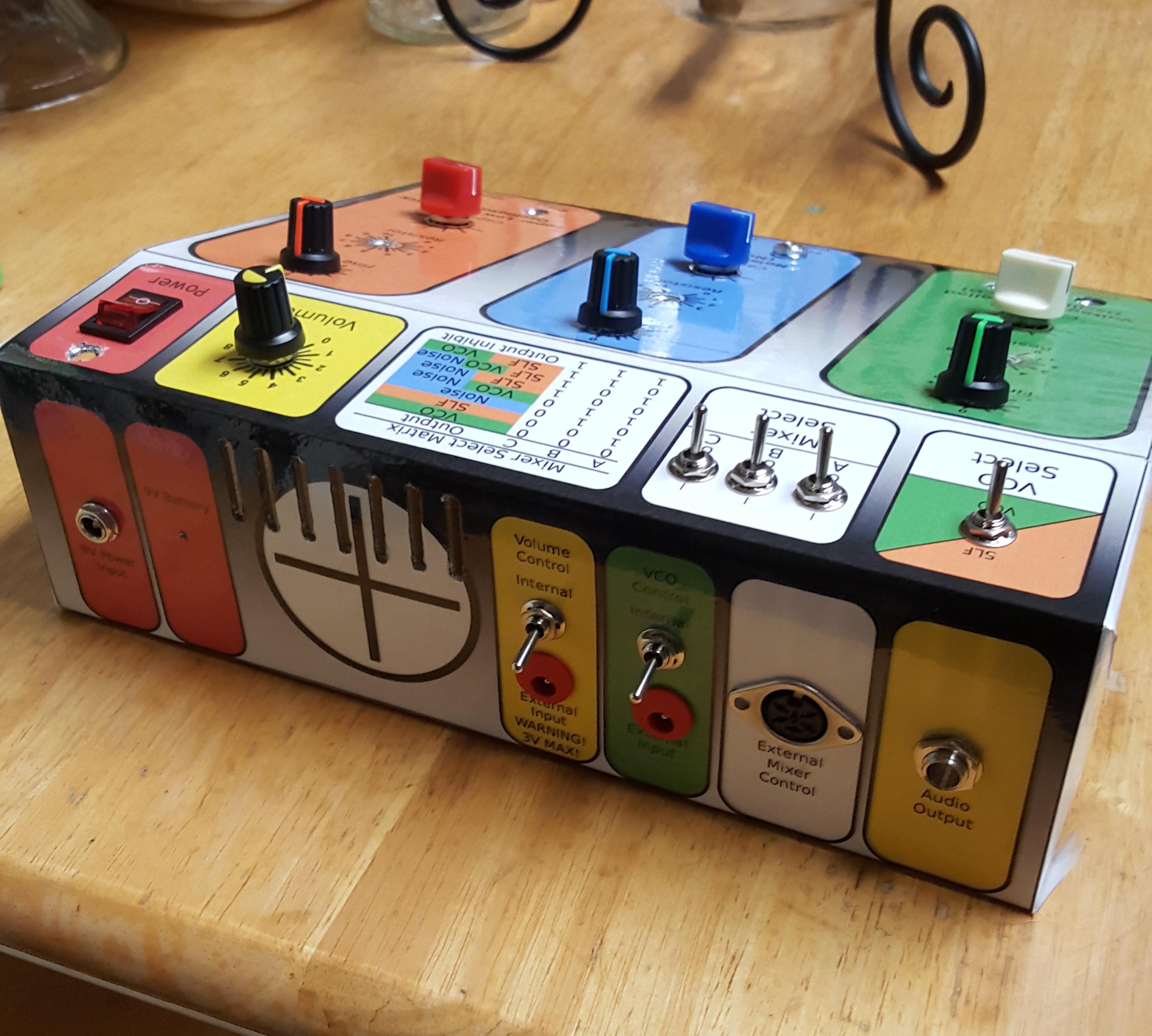
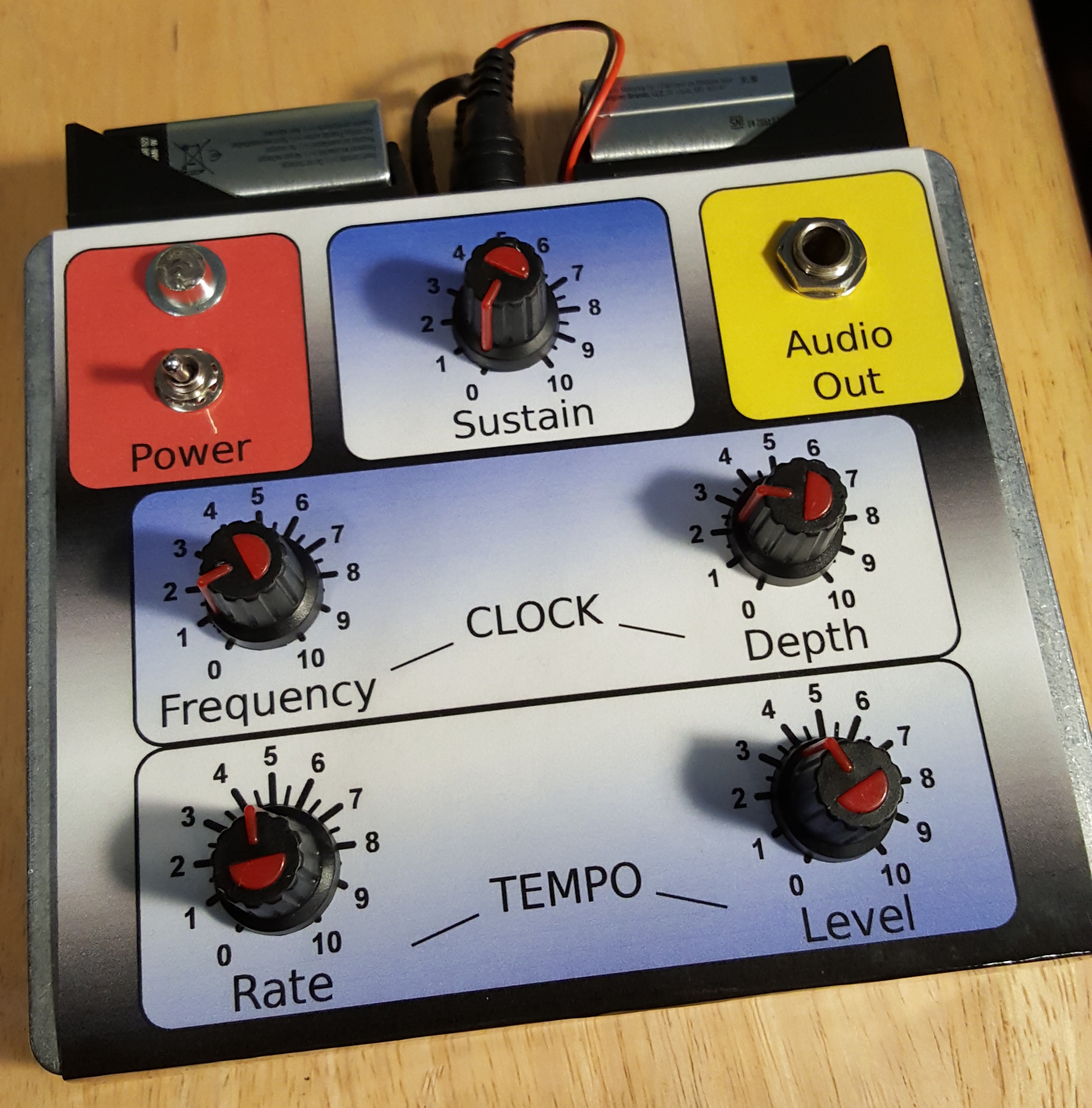
The enclosure (what you put your circuit in) is almost as important as the circuit board itself. Part of your initial design should probably take into account what type of box you'll be putting your project in. Some people like to build their own enclosures, and sometimes this is necessary. I spent a bit of time looking for the right shape and size of pre-built cases, but a few of mine cost over $30.00 each.
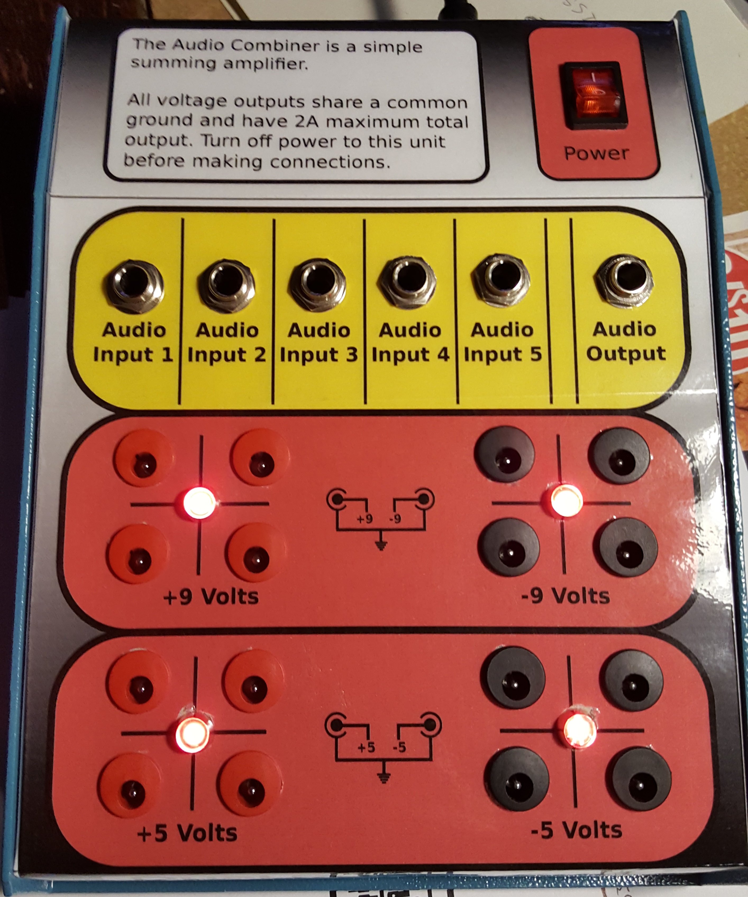
I was hoping to find a local shop that did laser etching for the case, but in the end, I just printed my panels on an inkjet printer, laminating them, and using the components to hold them in place (with a bit of gorilla-tape on the back)
The enclosures I bought range in price from $5.00-$35.00. The power supply enclosure was $30.00, the enclosure for the SN94281 was $33.00, and the box for the Audio Artist was $6.00.
If the enclosures aren't too large, the injet-laminator combo works prety well for these panel faceplates. There are other ways to do this, but none was as inexpensive as this for me. I have seen several methods for adding graphics and labels to panels, some involve decals, some are laser etched, and a few are CNC milled. Depending on your budget, you may opt for one of those methods.
Things to think about
Follow these steps, or use your own standards.
- Think about how many of the same board you may need. If you need 50, sending out will probably be cheaper and easier.
- If you're soldering this yourself, look for through-hole components. Surface mount is hard!
- Will you be sharing your circuit designs with others? Explain pinouts and components, either on the copper side or a silk layer
- If you don't need to etch that copper, save your solution! Mask large areas of the board, and make them ground planes if you'd like.